Open hardware
Your FPGA
in control of
your PCIe
Enter openPCIE backplane, the hardware backbone of PCIe systems built around your own plug-and-play host.
Most, if not all, commercial PCIe plug-in cards are wired as Endpoints. All PC mobos have their Root Complex soldered down, with their PCIe connectors designed to accept only the Endpoint plug-in cards. The two ends of the PCIe link indeed fully reinforce this state of affairs:
THE READILY AVAILABLE PCIe PLUG-IN CARDS ARE MADE TO BE ENDPOINTS. Period.
Why and When would you need this backplane?
- To test your Root Complex PCIe protocol stack using a standard EndPoint Slot or M.2 card.
- To build your custom PCIe embedded systems with plug-and-play (therefore easy) Host upgrades and repairs.
- For anything else that crosses your mind and puts your creativity and our card to good work.
Honestly, this piece of FR4 is unique.
We’ve spent a ton of time looking for a ready-made board in the likes of this backplane. Our original project goal was not to develop PCBs, but the RTL for an opensource PCIe RC and off-the-shelf Artix7 plug-in card.
Having found nothing on the civilian market, we bit the bullet and put in a bunch of extra work to design and validate this one-of-a-kind backplane — Not the VME/VPX, but a distant look in that direction, fully in opensource, ready for the makers, hobbyists, researchers, students, …
By Chili.CHIPS · Together with Envox d.o.o.
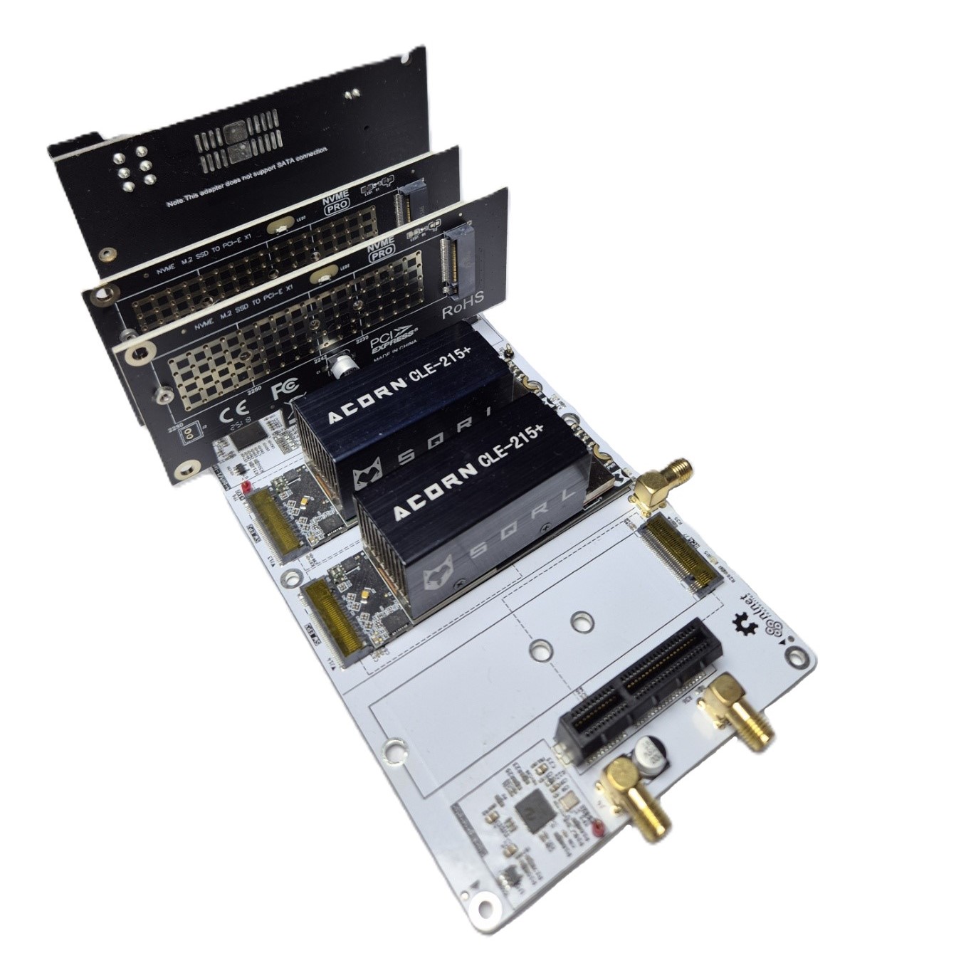
01 / The missing piece
Bring your PCIe host and peripherals. The backplane brings it all together.
All PCIe expansion cards expect a motherboard to be in charge. The motherboard supplies reference clock and reset. Its Root Complex discovers devices and manages communication. That works well when you are developing PCIe peripherals. Building a PCIe Host itself is a whole another game.
openPCIE provides the ecosystem that Endpoint cards need, and removes mobo RC out of the way. Plug-in an off-the-shelf FPGA card, load a Root Complex design into it, then plug-in an Endpoint. Or, yet better, load Endpoint bit file into the second, identical FPGA card. You can now develop for both ends of the link, inspect the transactions, experiment with software that controls them, …
The idea that makes it possible
An Endpoint card. A Root Complex role.
The RC connectors cross the Tx and Rx diff pairs, thus an ordinary plug-in card (= Endpoint pinout) can now be used as the Host. Clock and reset are supplied by our backplane.
The FPGA still needs RC stack and Host software — The connector wiring enables only the physical connection; it does not turn an arbitrary PCIe peripheral into a Host. But, our repo has fully worked out examples, along with sim setup, for both FPGA loads: RC and EP.
Our RC CPU is not an x86 or ARM. It is a soft RISC-V inside the FPGA. Still, you can plug-in the PC or RPi and have them take on the Host role instead of FPGA.
02 / One board. MULTIPLE ways to explore.
One-for-One and One-for-Four
The two logical PCIe islands share the infrastructure and provide separate PCIe data paths. Choose the topology that fits your needs.
POINT TO POINT ISLAND
Direct connection
An M.2 M-key Root Complex connector links directly to a standard PCIe Endpoint slot. This is the simplest and highest performing setup. We used it for initial testing of link training, enumeration and data transfer between two devices.
The direct connection has been successfully proven for Gen2 x4, with all four PCIe lanes active.
SWITCHED FABRIC ISLAND
Four downstream ports
An ASMedia ASM1184e PCIe 2.0 switch connects one upstream x1 link to four downstream x1 links. The provides two standard Slots and two M.2 M-key sockets.
All four ports share the upstream x1 bandwidth; adding ports does not multiply the host link’s capacity.
A closer look
Rx/Tx swap, Clock, Reset, Power
A common 12 V input feeds the board’s power conversion. The reference clock and reset circuits establish the operating environment for the plug-in devices.
The block diagram shows the connector roles and how both islands fit together. Open it at full size to inspect the details.
Open the full block diagram ↗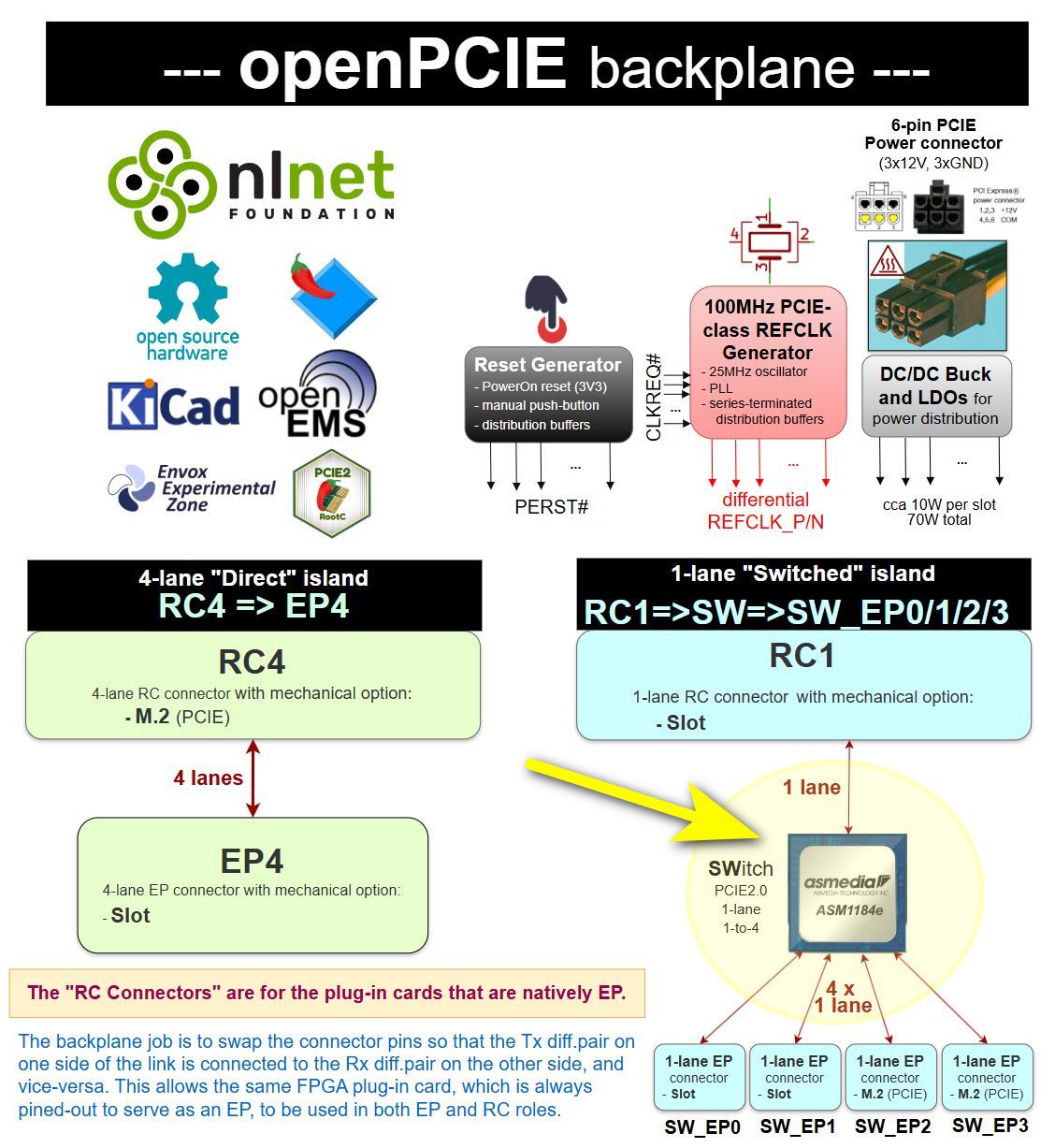
03 / What DO you WANT TO build?!
A jig for PCIe Hosts with non-host HW
01
Develop an FPGA Root Complex
Bring up a host design on a compatible FPGA, enumerate a peripheral and exercise Memory Read and Memory Write transactions. Use the direct island to keep the first experiments focused.
02
Connect a RISC-V system
Explore the broader openPCIE project’s soft RISC-V SoC, bare-metal driver and test application. Follow the path from software register accesses to PCIe traffic on real hardware.
03
Investigate switched systems
Add endpoints behind the ASM1184e and work through bridge discovery, resource assignment and shared upstream bandwidth. Device support depends on the host implementation and drivers.
04
Teach the complete stack
Give students access to the schematics, PCB, RTL, driver and simulation environment. Trace how power, reset, clocks, packets and software combine into a working system.
05
Evaluate interoperability
Use the backplane as a platform for planned cross-vendor work, including the related openCologne-PCIE Endpoint project. Compatibility must be established for each FPGA and configuration.
06
Extend a test setup
The repository also describes a PCIe jumper-cable approach for a conventional host. Follow its wiring and clocking requirements when exploring expansion or physical extension.
04 / Engineered in the open
The SI magic behind the connections
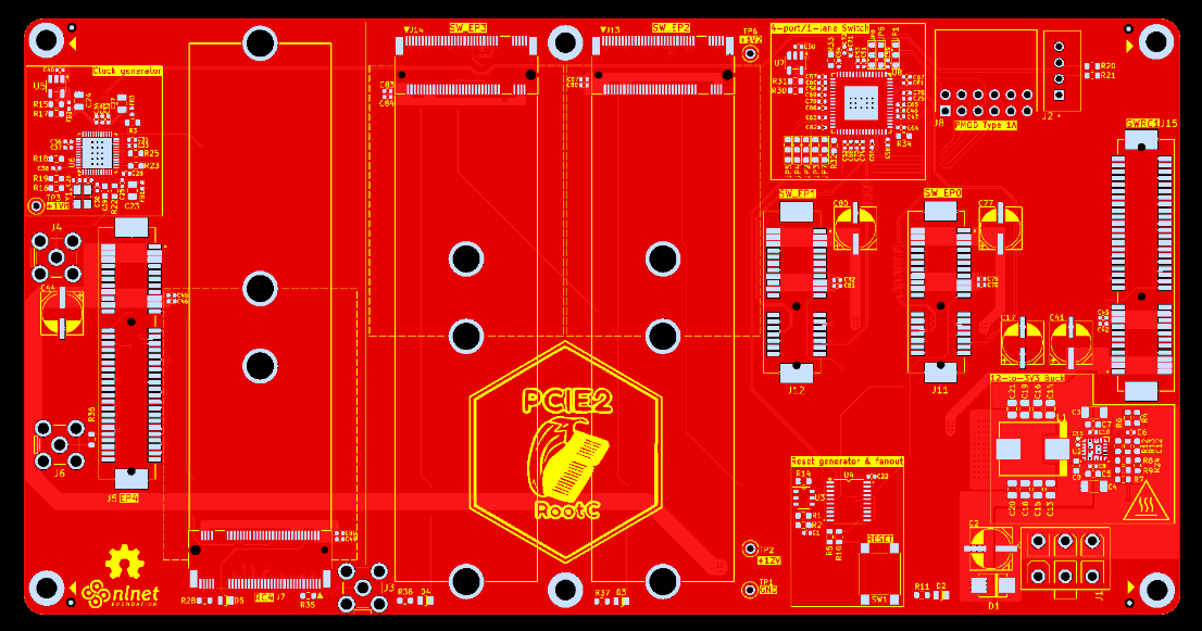
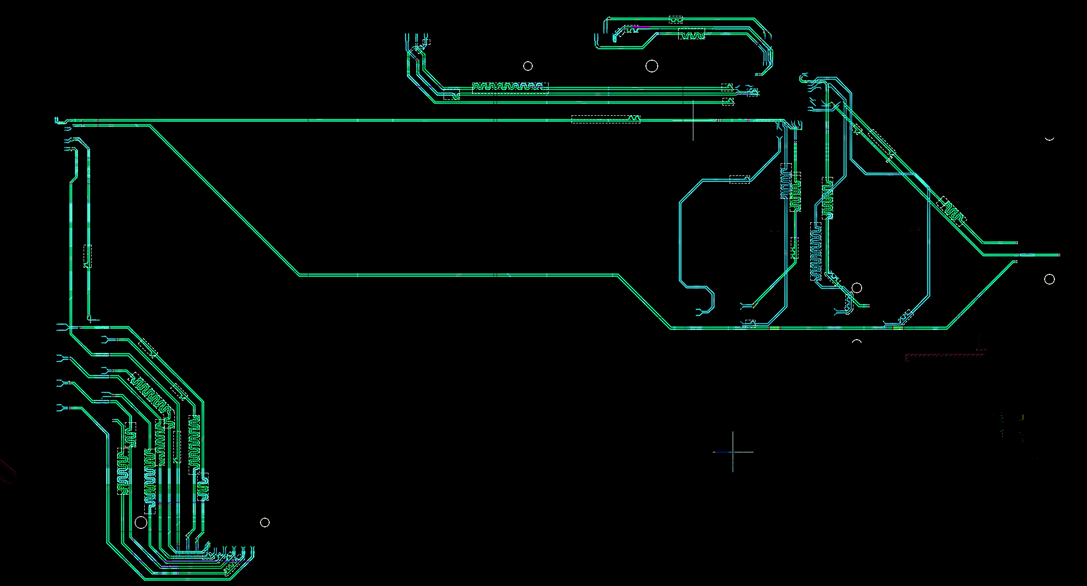
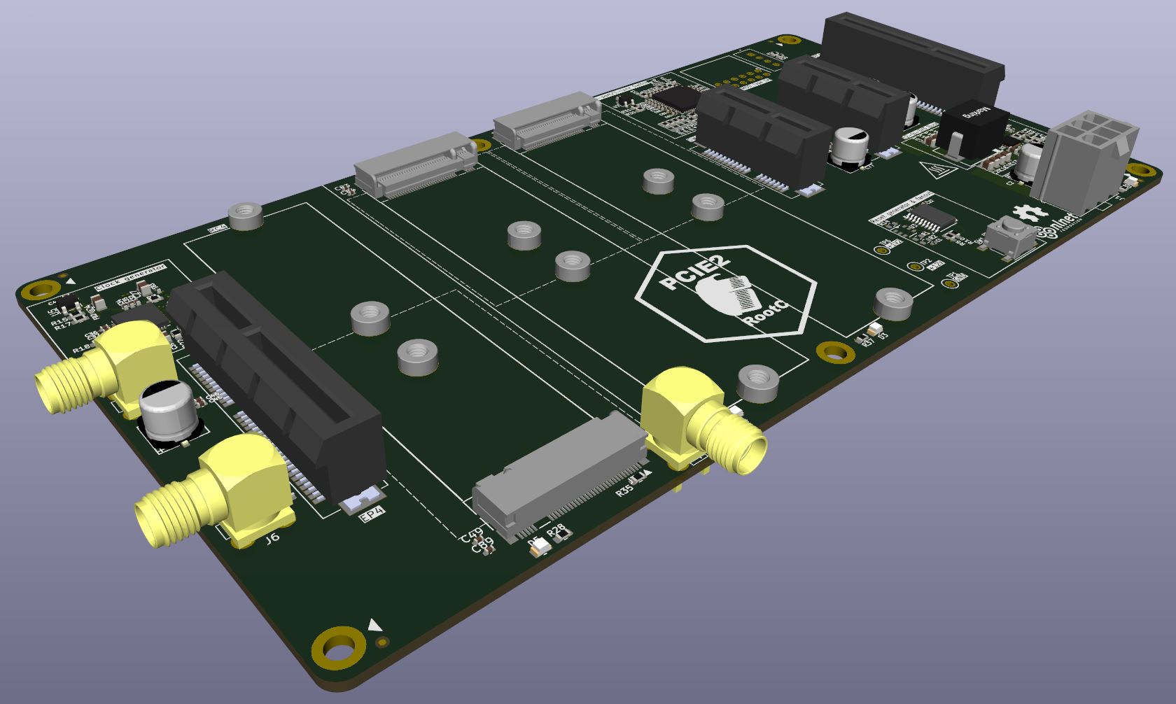
The KiCad design uses a four-layer stackup with ground and 3.3 V reference planes. High-speed differential pairs are routed as microstrips, with attention to skew, vias and connector stubs.
The PCB documentation specifies a 100 Ω ±10% differential-impedance target for data and clock signals and no more than 5 mil P-to-N skew. These are layout targets, not a substitute for measured compliance results.
A dedicated 100 MHz clock source and differential distribution support the cards. Clock-request handling and a push-button reset make repeated bring-up experiments practical.
05 / Hardware at a glance
Getting to knowing your backbone
| Feature | Documented design |
|---|---|
| Direct island | RC4 M.2 M-key to EP4 PCIe slot; four routed lanes. |
| Switched island | One upstream x1 link → four downstream x1 links through the ASMedia ASM1184e. |
| Endpoint connections | Direct: one PCIe slot. Switched: two PCIe slots and two M.2 M-key sockets. |
| Power input | Standard 6-pin PCIe connector carrying 12 V and ground. |
| Power budget | Approximately 70 W total; documentation gives a 10 W-per-slot guideline. Budget the complete system, including conversion losses. |
| Slot supplies | 12 V and 3.3 V as appropriate to the connector; onboard power conversion. |
| Reference clock | 100 MHz differential PCIe reference clock with clock-request handling. |
| Reset | PERST# distribution, supply supervision and manual reset button. |
| PCB | Four layers; KiCad 10.0.6 design files; impedance-controlled differential-pair routing. |
| Validated direct-link operation | Successful Gen2 x4 operation on the tested backplane configuration. |
| Hardware sources | Editable KiCad schematics and layout, schematic PDF, BOM and functional-test documentation. |
06 / From schematic to LIGHTS-up
Designed and Verified
CHECK 01
Power, reset and clocks
The prototype run included five boards manufactured by Elecrow. The project presentation reports successful factory checks of supply rails, manual reset distribution and the 25 MHz / 100 MHz clock signals.
CHECK 02
A working direct link
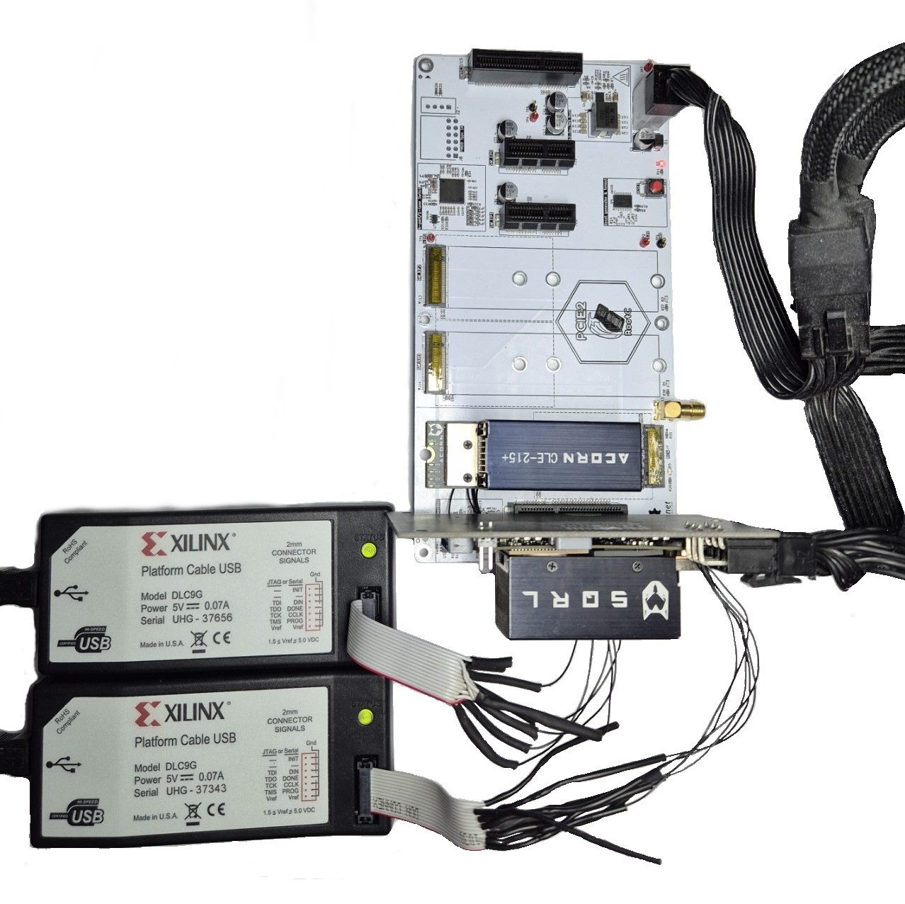
The project documents link establishment and payload transfer on physical FPGA hardware. Direct-link testing has also confirmed successful Gen2 x4 operation. The Endpoint LEDs display 0110, matching the decimal value 6 sent by the Root Complex.
CHECK 03
A better switch supply
Prototype testing exposed excessive heating around the switch’s 1.2 V LDO. The team reports that a buck-converter modification reduced the observed temperature to approximately 45 °C and restored stable communication. The published schematic includes a buck-based switch supply.
07 / Why this backplane?
Built for an unusual starting point
PCIe expanders already exist. What makes openPCIE different is its ability to operate an EP card as a RC, turning a peripheral into a host.
EXISTING HOST
Conventional PCIe expanders
Products such as Waveshare’s PCIe-Packet-Switch-4P expand a host connection into four Gen2 x1 sockets. That is useful when the host is already chosen and the goal is to attach more peripherals.
SINGLE-BOARD COMPUTER
Open Raspberry Pi hubs
The open PCIe3_Hub project is an example of an ASM2806-based design using Raspberry Pi 5 FPC connectors. It shows that openness alone is not the differentiator.
YOUR OWN HOST
The openPCIE approach
RC connector routing, onboard supporting circuits, a direct four-lane path and a separate switched island are combined for FPGA host experiments. The surrounding openPCIE project adds RTL, software and co-simulation to help you explore the whole system.
08 / On the bench
Real PCBs
09 / Open files. A complete starting point.
Going beyond the mere backplane
The backplane is part of a broader effort to open up the PCIe host stack. Read the design, study the implementation and adapt the pieces to your own experiments.
HARDWARE
Schematics, PCB and BOM
Browse the PCB source for KiCad files, the schematic PDF, bill of materials, component references and test procedure. The published schematic carries a CERN-OHL-P v2 notice.
LOGIC + SOFTWARE
Follow a PCIe transaction end-to-end
Explore the main project for the Artix-7 Root Complex work, a soft RISC-V SoC, bare-metal software, build instructions and the demonstration setup. Consult each file’s license when reusing it.
VERIFICATION
Simulate before the bench
Open the co-simulation environment to study the VProc / pcieVHost-based testbench and its CPU options. The current FPGA approach still uses AMD/Xilinx hard PCIe and transceiver blocks; removing those dependencies is a longer-term goal.
10 / Plan your setup
Bring your FPGA
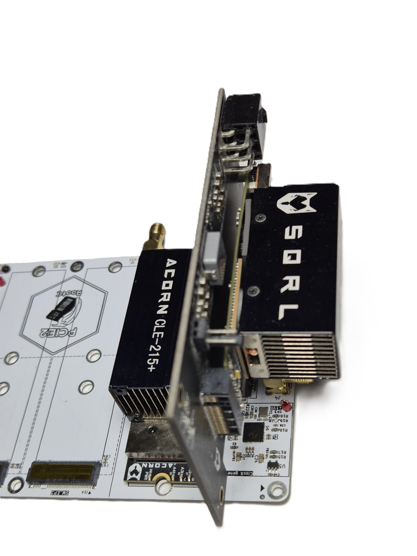
For a first direct-link experiment, plan for the backplane, a compatible RC-capable FPGA module, a suitable Endpoint, the required adapters, a correctly wired 12 V supply and a programming/debug connection. The repository demonstrates Acorn CLE-215+ modules and separate JTAG programmers.
Program the RC and EP designs, apply the documented reset sequence and verify link status before testing payload transfers. The driver and test application provide a starting point for enumeration and memory transactions.
Check clock-request wiring. The prototype report found that some older M.2-to-PCIe adapters did not carry CLKREQ#. Follow the documented solution for your exact board revision and adapter.
Before choosing cards
Form factor is only the first check. Confirm connector role, lane count, power budget, reference clock, reset behavior and software support.
Choose PCIe M-key devices supported by your FPGA host design and software.
The approximately 70 W total power budget is shared across the backplane and connected devices. Check each device’s power requirements when planning your setup.
11 / The next chapter
Bring openPCIE to your lab bench
We are preparing the next step for the openPCIE Backplane on Crowd Supply. Explore the working hardware and open documentation now, and check the campaign details here as they are finalized.
CROWD SUPPLY / CAMPAIGN DETAILS
Launch information
- Launch date
- [LAUNCH DATE — TO BE CONFIRMED]
- Campaign page
- [CROWD SUPPLY LINK — TO BE ADDED]
- Price & package contents
- [TO BE CONFIRMED]
- Estimated shipping
- [SHIPPING WINDOW — TO BE CONFIRMED]
These fields are placeholders for the campaign announcement. No orders or payments are collected on this page.
ACKNOWLEDGMENTS
openPCIE is developed by Chili.CHIPS*ba, with the backplane hardware developed by Envox and simulation contributions from wyvernSemi. The project acknowledges support from the NLnet Foundation through the NGI0 Core Fund, with funding from the European Commission’s Next Generation Internet programme under grant agreement No. 101092990.



PARTNERS









Chili.CHIPS / FPGA · Acceleration · Algorithms / Back to top ↑